It is important to know the materials of semiconductors in order to better understand them.
Therefore, this article introduces ‘silicon wafers’, which are the substrate material for semiconductors.
We start with the explanation of why silicon wafers are used in semiconductors and what processes are used to manufacture them.
This is the good introduction for those who want to learn more about semiconductors.
Contents
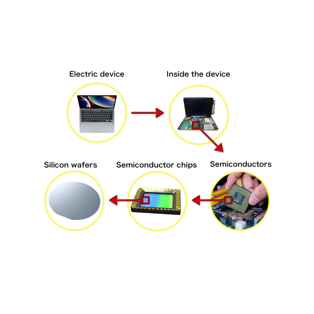
Semiconductors are made from ‘silicon wafers’.
Semiconductors are used in most electronic devices and the semiconductors themselves are made from ‘silicon wafers’ called eleven-nines.
The raw material, silicon, is 99.999999999% pure and its production is divided into several processes.
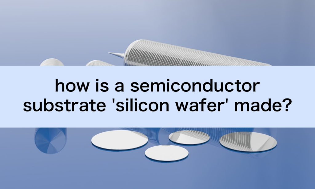
Even though it is used in most electronic equipment, we do not actually see it in our daily lives and it may be difficult to get an idea of it, so please see the diagram below.
When an electronic device is subdivided, semiconductors are embedded.
When the semiconductor is further subdivided, it contains a chip, and the ‘silicon wafer’ is the substrate for the chip.
As you see, there would be no semiconductors without silicon wafers.
It is no exaggeration to say that our lives have been enriched thanks to these substrates /silicon wafers.
Why are silicon wafers used in semiconductors?
There are several reasons why silicon wafers are used in the manufacture of semiconductors.
- Silicon is the second most abundant element on earth and is therefore a plentiful resource.
- It is easy to remove impurities and can be easily purified to high purity. Therefore, electron travel time is faster.
- Easy to control resistivity by adjusting the amount of impurities and single crystallization.
- Stable oxide film can be formed, and processing such as integration is easy.
Manufacturing process from wafer to semiconductor substrate, ‘silicon wafer’.
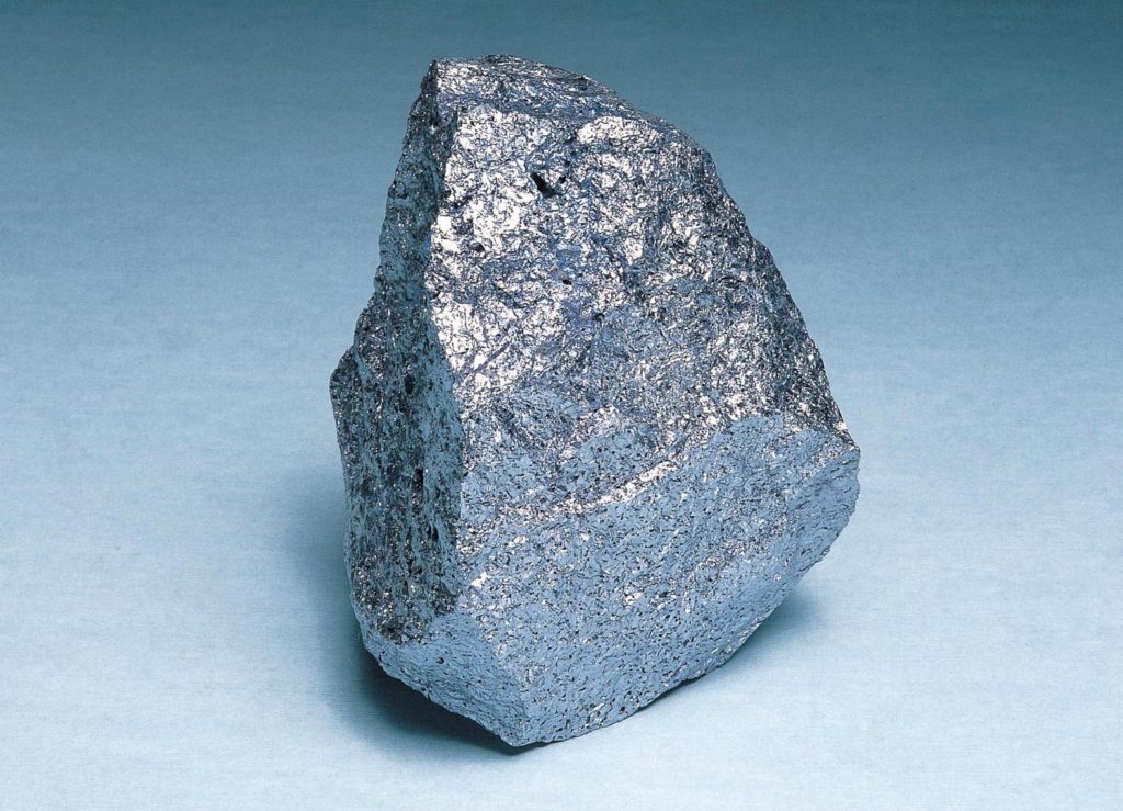
The raw material of wafers is ‘stone’.
Silica stone, a stone containing ‘silicon’, is ubiquitous on Earth.
The process of turning that silicon into “silicon wafers” is described below.
Silica stone ⇒ Metallic silicon ⇒ Polycrystalline silicon ⇒ Monocrystalline silicon ⇒ Silicon wafer
A reduction device called an arc furnace is used to produce 98 to 99% pure metallic silicon from silica stone.
The process incurs huge electricity costs.
The high cost of electricity in Japan makes it difficult to carry out such work, so the products are made in South-East Asia, where electricity costs are lower.
The process of polycrystalline silicon from metallic silicon produces even purer silicon, called “eleven nines”.
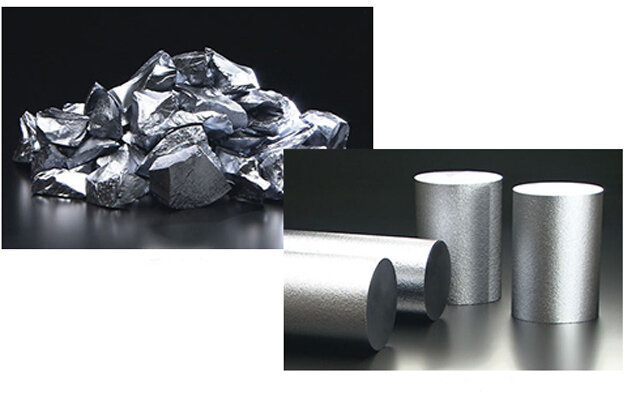
Polycrystalline silicon is produced from metallic silicon by a chemical reaction method (Simens method).
Most are produced in the USA.
Polycrystalline silicon is placed in a quartz crucible and melted into a sludge. Such sludge is then rotated and pulled upward to obtain monocrystalline silicon.
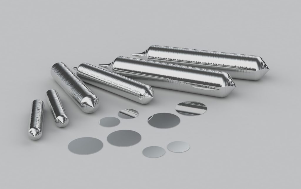
The bar-shaped monocrystalline silicon is cut into pieces about 1 mm thick with a high-speed wire.
The cut pieces are repeatedly polished and inspected to produce silicon wafers.
Summary.
In this article, we introduced the manufacturing process of silicon wafers, substrate of semiconductors.
Did you get the idea that semiconductors are produced through a series of small processes?
We offer the deposition test services using silicon wafers, so please feel free to contact us.