Contents
The global shortage of semiconductors has now taken its toll on many companies.
The situation is that high-performance electronic devices are becoming increasingly popular, and companies are scrambling for semiconductors to be used in their products.
One of the reasons for the shortage was the time it takes to produce semiconductors.
Semiconductors usually take more than three months from the time the materials are fed in until the completion of production.
Semiconductors are used in electronic equipment that undergo numerous processes to produce semiconductors that perform their functions perfectly.
Thin films are an essential technology for this process.
We will introduce the technology, equipment and methods of ‘thin films’, which are important for the semiconductor manufacturing process.
Basics of ‘thin films’ for semiconductor manufacturing.
A ‘thin film’ is a very thin, smooth film deposited on a glass or silicon substrate.
In a narrow sense, a thin film is a ‘film made by vacuum deposition technology, etc.’; in a broader sense, thin films made by plating or painting are also called ‘thin films’.
In the manufacture of semiconductors, fine circuits are made and thin films are processed into pattern shapes and stacked.
It is no exaggeration to say that semiconductors are made of thin films.
This article explains how thin a film needs to be to form a thin film.
Thin films are mainly films with a thickness of 10 µm (micrometers) or less.
A familiar example is paper.
Paper is approximately 60-70 µm (micrometers) thick.
Incidentally, aluminum foil is 10-60 µm.
In contrast, the thickness of thin films is a few nm (nanometer = 1/1000 micrometer), which is surprising!
If you are unsure of the units, please also refer to the unit conversion table below.
| 1meter | 0.001meter | 0.000001meter | 0.000000001meter |
|---|---|---|---|
| 1m | 0.001m | 0.000001m | 0.000000001m |
| 1,000mm | 1mm | 0.001mm | 0.000001mm |
| 1,000,000μm | 1,000μm | 1μm | 0.001μm |
Applications for forming thin films.
Various applications for forming thin films are utilized in addition to semiconductors.
Strengthening and protecting the surface of objects.
Molds and tools commonly used in manufacturing often have their surfaces protected by a hard thin film.
Control of light
The surface of metal products is often colored in various ways by means of thin films.
Thin films that reflect light well are also used around automobile headlight sources.
Integrated circuits at the heart of TVs, computers and smartphones
Integrated circuits (ICs) are complex electrical circuits trapped in a world so small that they can only be seen through a microscope.
They are manufactured using thin-film processing technology that utilizes a vacuum.
display device
Thin-film fabrication technology is generally the key technology for display devices such as display panels.
A variety of thin films are used here.
optical disk
Various compact discs and various digital discs are coated with a reflective film of aluminum.
Photovoltaic film
Amorphous silicon films, obtained by plasma chemical vapor deposition of a substance called silane gas, are used in solar cells.
Methods and techniques for making thin films.
There are several types of thin film formation, as shown in the diagram below.
| How to make thin films | Detail |
|---|---|
| evaporation method | This technique forms thin films by evaporating deposition materials such as metals and oxides in a vacuumed container and depositing them on the surfaces of opposing substrates. References※1.2.3.4 |
| Ion plating (IP) method | In principle, it is almost identical to the evaporation method, but the evaporation material is ionized by passing the evaporation particles through a plasma. A negative voltage is applied to the substrate to be deposited and the ionized deposition material is accelerated to impact the substrate to form a thin film. Ionization and acceleration can be used to create highly adherent films. References※1.5 |
| Sputtering method | Ions (usually Ar+ ions) created in the plasma by the discharge strike a plate (target) of the deposition material, which splashes the material. This is a method whereby the flung deposition material flies to the substrate to form a thin film. The sputtering method can be used for a wide range of deposition materials, such as metals and alloys with high melting points, which are difficult to deposit with the vapor deposition method. References※1.5.6 |
| Chemical vapor deposition (CVD) method | A method whereby gases containing the elements to be deposited are pumped onto the surface of a substrate and the films are deposited through chemical reactions and decomposition. There are different types of CVD, including thermal CVD, where the substrate is heated, and plasma CVD, where the reaction tube is depressurized and plasma is generated. References※1.7.8 |
| Atomic layer deposition (ALD) method | Although said to be a type of CVD, atomic layer deposition (ALD) is a method in which two or more types of raw material gases (precursor, precursor) are alternately introduced and exhausted to form a film by reacting the adsorbed raw material molecules on the surface of the deposited film. references※8.9 |
References
※1書籍「今日からモノ知りシリーズ トコトンやさしい真空の本」 p92-p93
※2尾池工業株式会社
※3コトバンク
※4ウィキペディア
※5東邦化研株式会社
※6尾池工業株式会社
※7ウィキペディア
※8化学的気相成長法の基本 論文
※9ウィキペディア
Various parameters that determine deposition conditions need to be controlled to achieve the appropriate film thickness and film condition.
In this light, it is clear that a lot of equipment is needed and technical know-how is important for the production of thin films.
Summary
In this article, basic knowledge of ‘thin films’ was introduced.
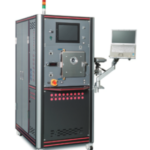
We manufacture equipment that is essential for forming thin films.
A wide range of vacuum equipment is available, including sputtering, ALD and evaporation systems.
For more information on the product, click here.