The ‘deposition’ technology is essential in the manufacturing process for the smartphones, PCs, cars, semiconductors and other products we use.
Invisible coating technologies support our daily lives.
As there are many different types of deposition, this article introduces a summary of the different types of deposition and their characteristics.
List of deposition types and characteristics
A variety of equipment and methods are available for deposition, including vapor deposition, sputtering and chemical vapor deposition (CVD) and spin coating.
Even in the deposition of the same substance, the properties may vary depending on the method used.
So it is necessary to know to some extent how different deposition methods affect film quality and properties.
Please refer to the list of deposition methods here.
of film How to make | detail |
|---|---|
evaporation method | This technique forms thin films by evaporating deposition materials such as metals and oxides in a vacuumed container and deposits them on the surfaces of opposing substrates. References※1.2.3.4 |
Ion plating (IP) method | In principle, it is almost identical to the evaporation method, but in this method, the evaporation material is ionized by passing the evaporation particles through plasma. A negative voltage is applied to the substrate to be deposited and the ionized deposition material is accelerated to impact the substrate to form a thin film. Ionization and acceleration can create highly adherent films. References※1.5 |
Sputtering method | Ions (usually Ar+ ions) created in the plasma by the discharge strike a plate (target) of the deposition material and splash the material. This is a method whereby the flung deposition material flies to the substrate to form a thin film. The sputtering method can be used for a wide range of deposition materials, such as metals and alloys with high melting points, which are difficult to deposit in case of vapor deposition method. References※1.5.6 |
Chemical vapor deposition (CVD) method | A method whereby gases containing the elements to be deposited are pumped onto the surface of a substrate and the films are deposited through chemical reactions and decomposition. There are different types of CVD, including thermal CVD, where the substrate is heated, and plasma CVD, where the reaction tube is depressurized and plasma is generated. References※1.7.8 |
Atomic layer deposition (ALD) method | Although said to be a type of CVD, atomic layer deposition (ALD) is a method in which two or more types of raw material gases (precursor, precursor) are alternately introduced and exhausted to form a film by reacting the adsorbed raw material molecules on the surface of the deposited film. references※8 |
References
※1 書籍「今日からモノ知りシリーズ トコトンやさしい真空の本」 p92-p93
※2 尾池工業株式会社
※3コトバンク
※4ウィキペディア
※5東邦化研株式会社
※6尾池工業株式会社
※7ウィキペディア
※8化学的気相成長法の基本 論文
※9ウィキペディア
In this article, we will discuss the typical deposition formation techniques mentioned above, namely chemical vapor deposition (CVD), atomic layer deposition (ALD) and sputtering, respectively.
Deposition method 1: CVD (chemical vapor deposition)
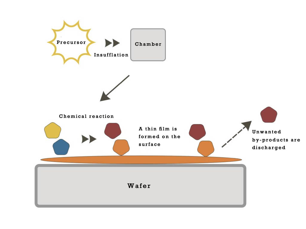
In chemical vapor deposition (CVD), chemical species are vaporized in a reaction to produce a thin film.
In this method, the precursor gas is transported onto the substrate and decomposed by a chemical reaction on the wafer.
This chemical reaction forms a thin film on the wafer surface and unwanted by-products are exhausted.
Deposition method 2: ALD (atomic layer deposition)

Atomic layer deposition is a method of forming very thin films by forming and stacking atomic layers one by one.
This deposition method is characterized by the sequential repetition of single, properly controlled steps.
In the first step, the wafer is covered with a precursor.
In a second step, another gas is introduced to react with the precursor, forming a film of material on the wafer surface.
ALD is a technology that has attracted a lot of attention in recent years due to the need for smaller, finer semiconductor elements.
Compared with CVD, it is characterized by high film pressure uniformity, atomic layer order thickness controllability and governability.
Deposition method 3: sputtering method

In sputtering, thin-film materials are deposited by bombarding the material to be thin-filmed with atoms or molecules that become ions and bounce off the material.
This technique is used to apply the bounced material to a substrate to form a thin film.
Sputtering equipment is needed to produce thin films using this sputtering phenomenon.
Sputtering equipment can achieve film deposition on materials such as metals and alloys with high melting points, which are difficult for the vacuum evaporation method.
Are you familiar with it? The principles of sputtering explained in simple terms.
Introduction to our deposition products.
We offer equipment for depositions.
Please check the range of products available for each of the deposition methods introduced above.
Summary
In this article, we introduced deposition, an important process in the process of making semiconductors and electronic devices.
We hope this is helpful, as the deposition method varies depending on the various types and substances in the deposition process.
We have been providing various deposition equipment for R&D. Please contact us through the following link if you are interested in our services,.