![Deposition? Sputtering? Semiconductors [insulators, conductors] that have radically changed the world.](https://agus.co.jp/en/wp-content/uploads/2023/09/image7-300x200-1.jpg)
Semiconductors are used all around us but do we really know what role they actually play and for what purpose they are used?
Contents
A semiconductor is something between an insulator and a conductor.
Semiconductors are ‘insulators’ that do not conduct electricity, but under certain conditions they are ‘conductors’ that do.
Its full name is ‘semiconductor integrated circuits’.
The binary system can be used because semiconductors can convey ‘0’ and ‘1’ information by conducting or not conducting electricity.
The binary system allows computers to perform various calculations.
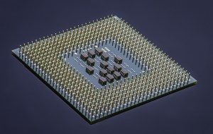
Typical materials used in semiconductors are silicon. This is where the name “Silicon Valley” originated.
Our life has changed drastically thanks to semiconductors, as silicon is abundant in the earth and semiconductors can be mass-produced.
The first product to use semiconductors was the transistor radio.

The binary system is a way of expressing numbers using only zeros and ones.
Example
| Decimal system | 0 | 1 | 2 | 3 | 4 | 5 | 6 | 7 | 8 |
| Binary system | 0 | 1 | 1 0 | 1 1 | 1 0 0 | 1 0 1 | 1 1 0 | 1 1 1 | 1 0 0 0 |
Semiconductors are vital to our lives!
Semiconductors used in familiar machines.

Temperature sensors in air conditioners are made of semiconductors.
The rice cooker’s heat regulation is controlled by semiconductors.

Semiconductors are also used in CPUs and SSDs in personal computers.

Semiconductors are also used in smartphones, digital cameras, washing machines, refrigerators, LED light bulbs, bank ATMs, trains, internet communications and other infrastructure, as well as in automobile engine control.
Semiconductors are used in various machines.
They are so commonplace that global giants such as Google, Apple, Facebook and Amazon cannot do anything without semiconductors.
In other words, a modern technological society would not be realized without semiconductors.
How do we make semiconductors? Sputtering method for making depositions.

There are several manufacturing processes involved in creating semiconductors, and this article describes sputtering as a deposition technique.
Deposition is a technique for attaching a thin film to the surface of an underlying material.
Deposition enables glass, resin and metal substrates to be equipped with functions such as current-carrying, light-controlling and heat-generating features.
The thickness of the membrane depends on the function of the membrane.
In this way, when deposited, the film can provide the necessary insulator and conductor functions for semiconductors.
There are several deposition methods.
Sputtering and evaporation methods are often used where optical films are required, such as lenses, etc.
Sputtering method
Suppose you throw a stone into a puddle of water. The water would then scatter and adhere to the prepared substrate.
Doing this in a vacuum is called the sputtering method.
Some more details.
A vacuum box filled with Ar (argon) gas contains an electron e-, and when e- is hit with argon, Ar+ is produced, which is called atomization.
Sputtering is a technique where atomized argon strikes a target and the atoms are knocked out, adhering to the substrate and creating a thin film.
*Argon has inert properties that does not react with other substances.
A clear explanatory video is below.
The principle is simple!
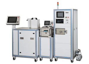
Equipment dedicated to sputtering

This is a deposition equipment that uses the sputtering phenomenon in which Ar ions collide with a target under a plasma discharge and the target material knocked out by the collision adheres to the opposing substrate.
A compact atomic layer deposition equipment for research and development, capable of uniform control of a single atomic layer, and of depositing films with high film quality and high step coverage.