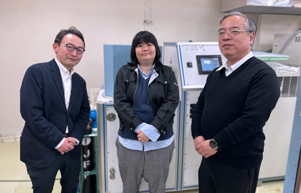
This time, we interviewed Prof. Kazuhisa Sueoka, chamberlain at Laboratory of Nanoelectronics, Graduate School of Information Science and Technology, Hokkaido University.
Professor Sueoka introduced the sputtering equipment for research in the field of electronics and material surface properties, and now uses it as collaborative equipment for the purpose of research with university students and/or other laboratories.
We received feedback on the actual experience with our sputtering system, how it differs from other company’s equipment and its advantages, so please take a look at this article if you are a researcher or university official currently considering obtaining this kind of equipment.
Contents
- 1 What research are you currently conducting?
- 2 What problems did you have before you got our sputtering system?
- 3 What triggered you to get our sputtering system ?
- 4 What are the advantages of getting our sputtering system ?
- 5 What do you currently use sputtering equipment for?
- 6 What do you think sputtering equipment will do for our lives in the future?
- 7 Conclusion
What research are you currently conducting?
Our research covers a wide variety of topics. It can be divided into three main areas.
The main research is the study of the physical properties of material surfaces using scanning tunneling microscopes and surface analyzers, such as atomic force microscopes, which examine the electronic, atomic and molecular states of material surfaces.
Fundamental research is also carried out to explore surface properties that can be used to express various electronics functions.
Firstly, we conduct research for the development of equipment, improving existing microscopes and devising original measurement methods.
Secondly we do in the field of nanomaterials such as graphene and carbon nanotubes, which can be applied to sensors and solar cells.
Lastly we do for a three-pronged research program, which investigates the properties of organic thin films and their application in the field of electronics.
As this research is a fundamental part of the electronics field, it can be the base for other researches
What problems did you have before you got our sputtering system?
Sputtering equipment is versatile and has been used in this laboratory for about 30 years..
But if it’s older, we’ve had problems with the equipment being less user-friendly and less versatile.

What triggered you to get our sputtering system ?
We had a history of working with Suga Co., Ltd. on research, having previously worked together to fabricate sputtering equipment for special applications.
It was sputtering equipment only for limited applications, although research has progressed,
the need for more general-purpose sputtering equipment has been arisen.
Suga offers good after-sales service, and they consult with us on details that other companies don’t respond. As such, we internally agreed that we would continue to work with
Suga Co., Ltd. ,when we got to purchase highly versatile sputtering equipment.
Suga has good technical skills and fabricate compact and beautiful equipment.
Universities have limited physical area, their design fitting to the limited space is really of help to us..
It’s not easy to ask a big company to do this because they often have to divert existing ones.
What are the advantages of getting our sputtering system ?

Firstly, user friendly was the first point..
It has few operating peculiarities and is simple enough for university students to handle and is used in many student research projects.
Not only in my laboratory, but also in other laboratories, we use it in a wide range of fields as shared equipment at Hokkaido University.
Secondly, the very easy maintenance of the system is the second point where the introduction of the system was a good decision.
Sputtering equipment tends to be complex, but Suga’s sputtering equipment is designed to be as simple as possible and easy handling even for a woman. I really appreciated the fact that maintenance can be easily done as long as we have knowledge.
Finally, the user-friendly nature of the system is one of the reasons why I am satisfied with Suga Co., Ltd..
From the design stage of the sputtering equipment, Suga makes it easy for us to use and maintain.
So they make the equipment easy to use at site.
If it were true, we would like to ask AGUS to do the maintenance, but the university’s research funding is limited, we often have to repair the equipment on our own.
However, when we had problems, we were able to fix the equipment via video call while you showed us where the equipment was repaired, so you have provided us with very generous after-sales service and support.
What do you currently use sputtering equipment for?
When trying to investigate electrical movement, electrodes that conduct electricity are inevitably needed.
Sputtering equipment is often essential, as sputtering equipment must be used for its electrodes.
As it is an essential piece of equipment for cutting-edge research, it is often booked up for use within the university.
What do you think sputtering equipment will do for our lives in the future?
It is always necessary for research and development in electronics and is useful in a wide range of fields, including satellite components in the field of space engineering, familiar electronic components such as memories and processors, and biotechnology, to name but a few.
The sputtering equipment is “essential to the roots” of research in many fields, so it is equipment that we will not be able to do without in the future.
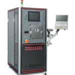
Introduction of SUGA’s sputtering equipment

The sputtering equipment delivered by SUGA to the Laboratory of Nanoelectronics, Graduate School of Information Science and Technology, Hokkaido University is “SSP3000Plus”.
Main features
- High performance model with 3-way cathode
- Film thickness distribution within φ100mm is less than ±3
- Connectable to other Plus series equipment
For details, please click here.
Conclusion
Professor Sueoka gave us a firsthand account of his experience using SUGA’s sputtering equipment.
He gave high marks not only for the simplicity of equipment operation and ease of maintenance, but also for the fact that staff of SUGA incorporated his requests from the design stage and provided consultation on customization according to his research objectives and on-site conditions.
We, SUGA is committed to meeting the various needs of our customers to ensure that they are satisfied with our products even after purchase.
We hope that this can be one of the good decision-making factors for those who are thinking about purchasing our products. Furthermore, we have branches in Sapporo and Shizuoka, and can provide a support promptly anywhere in Japan.
Please contact us in below.