AFM (Atomic Force Microscopy) is a microscope that uses atomic force.
AFM is a microscope that uses atomic forces to observe surface topography.
This microscope is most often utilised in SPM, as it allows high-resolution observation of samples in air and without treatment.
One of its strengths is that, unlike STM (scanning tunneling microscopy), it can measure conductors, semiconductors and insulators without distinction.
The disadvantage is that a normal AFM couldn’t make videos because it would take several minutes to create a single image.
However, it’s now possible to make movies after the recent creation of ‘high-speed AFM’.
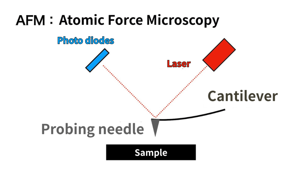
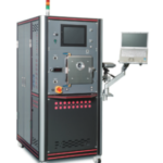
Structure of AFM (Atomic Force Microscopy).
The method involves placing the sample on a stage (platform) and measuring its shape using a needle or laser.
The needle and sample repel each other by making each a + charge.
The stage leaves the surface at the moment repulsive force is generated, allowing the surface to be measured without damaging the sample.
By shining a laser onto a cantilever (a plate with a needle attached), the cantilever deforms, causing the laser’s reflection angle to change, which allows the shape to be measured.
What can be observed with AFM (Atomic Force Microscopy)
AFM is a microscope capable of visualizing surface topography at the nanoscale. It enables not only the observation of surface structures but also the evaluation of a wide range of properties, including material hardness and electrical resistance.
Here, we will examine in detail what kind of information can be obtained with AFM, broken down by specific measurement parameters.
Surface structure of objects
AFM enables measurement of surface roughness on various materials, processed items, and molded objects.
Evaluating surface roughness is a critical process directly linked not only to managing finish uniformity and appearance quality but also to improving product lifespan, friction characteristics, and mechanical efficiency.
For example, it can be utilized for a wide range of evaluations, including the reflective properties of gloss finishes, the airtightness of packaging, the texture of embossed finishes, the friction force of clutches and valves, the adhesion of substrates and plating, the print quality of printed paper, and the performance of optical components.
Material hardness
AFM measures mechanical properties such as elastic modulus and viscoelasticity, enabling detailed evaluation of a material’s “hardness” and its response to applied force.
Elastic modulus indicates a material’s “resistance to deformation” when subjected to external force; a higher value signifies a harder material that resists deformation.
Conversely, viscoelasticity indicates a material’s “stickiness” and “tendency to return to its original state,” which is useful in analyzing shock absorption and energy transfer.
Measuring these properties is valuable for material design where both strength and flexibility are required, such as in tires.
Electrical resistance
AFM can measure not only surface structures but also current resistance values.
Materials with higher resistance allow current to flow less easily, while materials with lower resistance allow current to flow more readily.
In particular, materials with low resistance values exhibit high antistatic properties, making them more effective at preventing electrostatic discharge damage.
Evaluating electrical resistance with AFM is a crucial technique applicable to a wide range of product designs, including quality control for electronic components and conductive materials, as well as the development of antistatic materials.
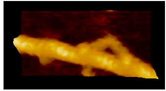
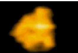
Real image samples from AFM (Atomic Force Microscopy).
AFM can also observe non-conductive materials and is used in various fields.
The following sections will show you the images together with a picture.
Two measurement modes of AFM (Atomic Force Microscopy)
AFM measurement modes are broadly categorized into the following two types:
・Contact Mode
・Dynamic Mode
Let’s examine them in detail in the next section.
Contact Mode
Contact mode is used to evaluate the surface topography of relatively hard materials.
In this method, the probe (cantilever tip) scans while maintaining constant contact with the sample surface. The resulting deflection is detected to measure the surface topography.
While its principle is simple and it readily achieves high resolution, continuous contact between the probe and sample generates friction and it can potentially damage soft materials.
Dynamic Mode
In Dynamic Mode, the cantilever is vibrated near its resonance frequency while measuring the sample surface.
The height is automatically controlled to maintain a constant amplitude change caused by the probe interacting with the sample.
Compared to contact mode, it causes less damage to the sample. Furthermore, using a stiffer cantilever offers the advantage of suppressing the effects of static electricity.
Another characteristic is the ability to obtain information about viscoelasticity from the acquired phase signal.
History of AFM (Atomic Force Microscopy)
Originally, the ‘STM: Scanning Tunneling Microscope’ was developed to observe on the sample surface.
However, STM has the disadvantage that only conductive samples can be observed, as the surface is observed by detecting tunneling currents.
Therefore, in 1986, Dr ‘Gerd Beinig’, Dr ‘Calvin Quart’ and others developed the AFM, which converts interatomic energy into electrical signals, and has been used to this day.
Summary
In this article, we explained AFM (Atomic Force Microscopy).
Finally, let’s look back at the key points.
・AFM is a microscope that uses atomic forces to measure the unevenness of a sample surface by cantilever distortion and laser reflection.
・Non-conductive materials that could not be realised by STM can be measure
・Previously only images were available, but with the birth of high-speed AFM, it is now possible to make movies.
・AFM was developed in 1986.
We mentioned at the beginning that AFM is a type of SPM (scanning probe microscope).
For more information on SPM, see also the following article.