
STM (scanning tunneling microscope) is a type of SPM (scanning probe microscope).
If you would like to know more about SPM, please read the following article, which also explains it.
This article provides a simple explanation of how STMs observe samples.
We hope that you will find this information useful, as we can only provide it because we are usually involved in work related to atoms.
Let’s look at it.
Contents
STM (scanning tunneling microscope) is a microscope that uses tunneling currents.

STM is a microscope that observes surface irregularities by detecting tunneling currents between a metal probe and a conductive sample.
The multi-probe scanning tunneling microscopes, one of the STMs, use several needles and can characterize Nano scale samples.
As well as measuring surfaces, it also has the feature of being able to process individual atoms, enabling sample surfaces to be processed at the nanometer level.
The disadvantage is that, as it uses tunneling currents, materials that do not conduct current cannot be measured.
AFM (Atomic Force Microscopy)is used to measure conductive materials.
Structures of STM (Scanning Tunneling Microscope).
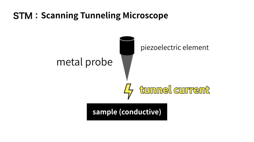
Piezoelectric elements are used in the cantilever to which the STM probe is attached.
The system is based on a piezo element that is distorted by applying a voltage to it, and by adjusting the distance between the needle and the sample, the unevenness of the sample surface can be detected.
The further away the sample and needle are, the weaker the tunneling current becomes, and the closer they are, the stronger the tunneling current becomes.
The method is to measure the size of the surface by returning it to its initial position in relation to the strength of this current.
Real image sample of STM (Scanning Tunneling Microscope).
A STM allows you to see atoms down to the size of a grain.
Looking at the real image samples, you can see the connections between atoms and clearly see what is shown in the image diagrams in textbooks.
For a sample of the actual image, please see the following pages.
Scanning Tunneling Microscope (STM)
History of STM (scanning tunneling microscopy)

The STM is the oldest microscope of its kind, the scanning probe microscope.
Developed in 1981 by Dr ‘Gerd Beinig’ and Dr ‘Heinrich Rohrer’ at the IBM Zurich Research Institute.
It was a revolutionary microscope that could not only measure surfaces but also process atoms, but it also had the disadvantage that it could not measure non-conductive materials.
This shortcoming was the seed for the later development of the atomic force microscope (AFM).
Summary
In this article, we explained STM (Scanning Tunneling Microscopy).
Finally, let’s look back at the key points.
・STM is a microscope that uses tunneling currents generated between a metal probe and a conductive material to measure the unevenness of a sample surface
・Other probe scanning tunneling microscopes can also measure the characteristics
・Not only can surfaces be measured, but also each atom can be processed
・It has the disadvantage that only conductive substances can be measured.
・STM was developed in 1981.
We mentioned at the beginning that STM is a type of SPM (scanning probe microscope).
If you would like to know more about SPM, please read the following article, which also explains it.