Explanation of the differences between ALD,…
The 'deposition' technology is essential in the manufacturing process for the smartphones, PCs, cars, semiconductors and other products we use.
The 'deposition' technology is essential in the manufacturing process for the smartphones, PCs, cars, semiconductors and other products we use.
Relationship between sputter deposition and substrate temperature. Did you know that the substrate on which the film is deposited is also heat

Test example of deposition We have experimented with the SSP1000 cubic sputtering system to see if it is possible to sputter deposition wi
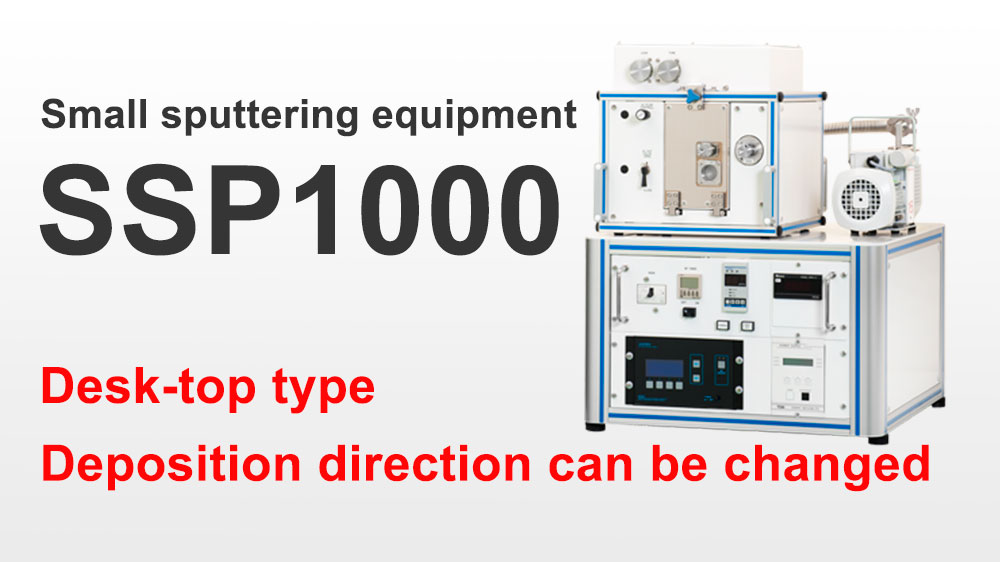
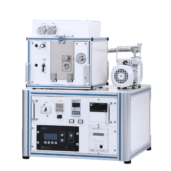
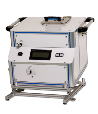
We introduce a desk model recommended point to be able to make the placement change into.Desk-top type model can allow you to make a flexible lay
TiN is commonly deposited for semiconductors as the barrier layer in between Oxide film layer (SiO2, etc.) and Cupper to prevent the integration.
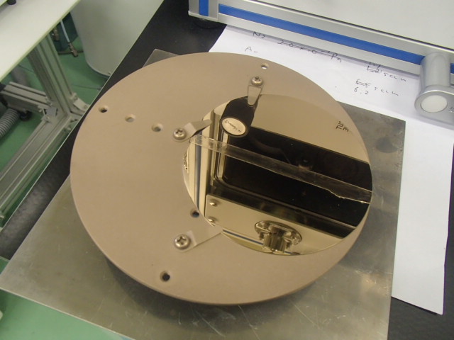
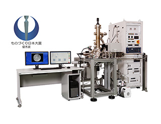
Photo Emission Electron Microscopy (PEEM)
2 dimensions mapping can be performed in real time to see the status of the electron (work function) on the surface of the sample.
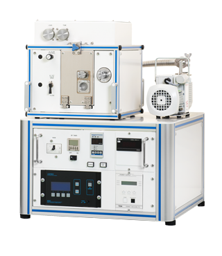
Desk-Top model as a low end model and it can select the deposition direction.
Triple cathode, substrate heating MAX800 ℃, film thickness distribution ± 3%
Triple cathode, substrate heating up to Max.800℃, film thickness distribution ±3%, Expandable type.
This model is capable of depositing all over the surface for both powder and solid particles.
© 2024 SUGA Co., Ltd. All Rights Reserved.